The Intel 8008 ("eight-thousand-eight" or "eighty-oh-eight") is an early 8-bit microprocessor capable of addressing 16 KB of memory, introduced in April 1972. The 8008 architecture was designed by Computer Terminal Corporation (CTC) and was implemented and manufactured by Intel. While the 8008 was originally designed for use in CTC's Datapoint 2200 programmable terminal, an agreement between CTC and Intel permitted Intel to market the chip to other customers after Seiko expressed an interest in using it for a calculator.
 An Intel C8008-1 processor variant with purple ceramic, gold-plated metal lid and pins. | |
| General information | |
|---|---|
| Launched | April 1972 |
| Discontinued | 1983[1] |
| Marketed by | Intel |
| Designed by | Computer Terminal Corporation (CTC) |
| Common manufacturer(s) |
|
| Performance | |
| Max. CPU clock rate | 500 kHz to 800 kHz |
| Data width | 8 bits |
| Address width | 14 bits |
| Architecture and classification | |
| Application | Computer terminals, calculators, bottling machines, 1970s ASEA industrial robots[2] (IRB 6), simple computers, etc. |
| Technology node | 10 µm |
| Instruction set | 8008 |
| Physical specifications | |
| Transistors |
|
| Package(s) |
|
| Socket(s) | |
| History | |
| Successor(s) | Intel 8080 |
| Support status | |
| Unsupported | |
History edit
In order to address several issues with the Datapoint 3300, including excessive heat radiation, Computer Terminal Corporation (CTC) designed the architecture of the 3300's planned successor with a CPU as part of the internal circuitry re-implemented on a single chip. Looking for a company able to produce their chip design, CTC co-founder Austin O. "Gus" Roche turned to Intel, then primarily a vendor of memory chips.[3] Roche met with Bob Noyce, who expressed concern with the concept; John Frassanito recalls that:
"Noyce said it was an intriguing idea, and that Intel could do it, but it would be a dumb move. He said that if you have a computer chip, you can only sell one chip per computer, while with memory, you can sell hundreds of chips per computer."[3]
Another major concern was that Intel's existing customer base purchased their memory chips for use with their own processor designs; if Intel introduced their own processor, they might be seen as a competitor, and their customers might look elsewhere for memory. Nevertheless, Noyce agreed to a US$50,000 development contract in early 1970 (equivalent to $392,000 in 2023). Texas Instruments (TI) was also brought in as a second supplier.[citation needed]
TI was able to make samples of the 1201 based on Intel drawings,[citation needed] but these proved to be buggy and were rejected. Intel's own versions were delayed. CTC decided to re-implement the new version of the terminal using discrete TTL instead of waiting for a single-chip CPU. The new system was released as the Datapoint 2200 in the spring 1970, with their first sale to General Mills on 25 May 1970.[3] CTC paused development of the 1201 after the 2200 was released, as it was no longer needed. Six months later, Seiko approached Intel, expressing an interest in using the 1201 in a scientific calculator, likely after seeing the success of the simpler Intel 4004 used by Busicom in their business calculators. A small re-design followed, under the leadership of Federico Faggin, the designer of the 4004, now project leader of the 1201, expanding from a 16-pin to 18-pin design, and the new 1201 was delivered to CTC in late 1971.[3]
By that point, CTC had once again moved on, this time to the Datapoint 2200 II, which was faster. The 1201 was no longer powerful enough for the new model. CTC voted to end their involvement with the 1201, leaving the design's intellectual property to Intel instead of paying the $50,000 contract. Intel renamed it the 8008 and put it in their catalog in April 1972 priced at US$120 (equivalent to $874 in 2023). This renaming tried to ride off the success of the 4004 chip, by presenting the 8008 as simply a 4 to 8 port, but the 8008 is not based on the 4004.[4] The 8008 went on to be a commercially successful design. This was followed by the Intel 8080, and then the hugely successful Intel x86 family.[3]
One of the first teams to build a complete system around the 8008 was Bill Pentz' team at California State University, Sacramento. The Sac State 8008 was possibly the first true microcomputer, with a disk operating system built with IBM Basic assembly language in PROM, all driving a color display, hard drive, keyboard, modem, audio/paper tape reader, and printer.[5] The project started in the spring of 1972, and with key help from Tektronix, the system was fully functional a year later. Bill assisted Intel with the MCS-8 kit and provided key input to the Intel 8080 instruction set, which helped make it useful for the industry and hobbyists.[citation needed]
In the UK, a team at S. E. Laboratories Engineering (EMI) led by Tom Spink in 1972 built a microcomputer based on a pre-release sample of the 8008. Joe Hardman extended the chip with an external stack. This, among other things, gave it power-fail save and recovery. Joe also developed a direct screen printer. The operating system was written using a meta-assembler developed by L. Crawford and J. Parnell for a Digital Equipment Corporation PDP-11.[6] The operating system was burnt into a PROM. It was interrupt-driven, queued, and based on a fixed page size for programs and data. An operational prototype was prepared for management, who decided not to continue with the project.[citation needed]
The 8008 was the CPU for the very first commercial non-calculator personal computers (excluding the Datapoint 2200 itself): the US SCELBI kit and the pre-built French Micral N and Canadian MCM/70. It was also the controlling microprocessor for the first several models in Hewlett-Packard's 2640 family of computer terminals.[citation needed]
In 1973, Intel offered an instruction set simulator for the 8008 named INTERP/8.[7] It was written in FORTRAN IV by Gary Kildall while he worked as a consultant for Intel.[8][9]
Design edit

| 13 | 12 | 11 | 10 | 09 | 08 | 07 | 06 | 05 | 04 | 03 | 02 | 01 | 00 | (bit position) |
| Main registers | ||||||||||||||
| A | Accumulator | |||||||||||||
| B | B register | |||||||||||||
| C | C register | |||||||||||||
| D | D register | |||||||||||||
| E | E register | |||||||||||||
| H | H register (indirect) | |||||||||||||
| L | L register (indirect) | |||||||||||||
| Program counter | ||||||||||||||
| PC | Program Counter | |||||||||||||
| Push-down address call stack | ||||||||||||||
| AS | Call level 1 | |||||||||||||
| AS | Call level 2 | |||||||||||||
| AS | Call level 3 | |||||||||||||
| AS | Call level 4 | |||||||||||||
| AS | Call level 5 | |||||||||||||
| AS | Call level 6 | |||||||||||||
| AS | Call level 7 | |||||||||||||
| Flags | ||||||||||||||
| C | P | Z | S | Flags[10][a] | ||||||||||
The 8008 was implemented in 10 μm silicon-gate enhancement-mode PMOS logic. Initial versions could work at clock frequencies up to 0.5 MHz. This was later increased in the 8008-1 to a specified maximum of 0.8 MHz. Instructions take between 5 and 11 T-states, where each T-state is 2 clock cycles.[11]Register–register loads and ALU operations take 5T (20 μs at 0.5 MHz), register–memory 8T (32 μs), while calls and jumps (when taken) take 11 T-states (44 μs).[12]The 8008 is a little slower in terms of instructions per second (36,000 to 80,000 at 0.8 MHz) than the 4-bit Intel 4004 and Intel 4040.[13] but since the 8008 processes data 8 bits at a time and can access significantly more RAM, in most applications it has a significant speed advantage over these processors. The 8008 has 3,500 transistors.[14][15][16]
The chip, limited by its 18-pin DIP, has a single 8-bit bus working triple duty to transfer 8 data bits, 14 address bits, and two status bits. The small package requires about 30 TTL support chips to interface to memory.[17] For example, the 14-bit address, which can access "16 K × 8 bits of memory", needs to be latched by some of this logic into an external memory address register (MAR). The 8008 can access 8 input ports and 24 output ports.[11]
For controller and CRT terminal use, this is an acceptable design, but it is rather cumbersome to use for most other tasks, at least compared to the next generations of microprocessors. A few early computer designs were based on it, but most would use the later and greatly improved Intel 8080 instead.[citation needed]
Related processor designs edit
The subsequent 40-pin NMOS Intel 8080 expanded upon the 8008 registers and instruction set and implements a more efficient external bus interface (using the 22 additional pins). Despite a close architectural relationship, the 8080 was not made binary compatible with the 8008, so an 8008 program would not run on an 8080. However, as two different assembly syntaxes were used by Intel at the time, the 8080 could be used in an 8008 assembly-language backward-compatible fashion.[18][irrelevant citation]
The Intel 8085 is an electrically modernized version of the 8080 that uses depletion-mode transistors and also added two new instructions.[19][irrelevant citation]
The Intel 8086, the original x86 processor, is a non-strict extension of the 8080, so it loosely resembles the original Datapoint 2200 design as well. Almost every Datapoint 2200 and 8008 instruction has an equivalent not only in the instruction set of the 8080, 8085, and Z80, but also in the instruction set of modern x86 processors (although the instruction encodings are different).[20][irrelevant citation]
Features edit
The 8008 architecture includes the following features:[citation needed]
- Seven 8-bit "scratchpad" registers: The main accumulator (A) and six other registers (B, C, D, E, H, and L).
- 14-bit program counter (PC).
- Seven-level push-down address call stack. Eight registers are actually used, with the top-most register being the PC.
- Four condition code status flags: carry (C), even parity (P), zero (Z), and sign (S).
- Indirect memory access using the H and L registers (HL) as a 14-bit data pointer (the upper two bits are ignored).
Instruction Set edit
Instructions are all one to three bytes long, consisting of an initial opcode byte, followed by up to two bytes of operands which can be an immediate operand or a program address. Instructions operate on 8-bits only; there are no 16-bit operations. There is only one mechanism to address data memory: indirect addressing pointed to by a concatenation of the H and L registers, referenced as M. The 8008 does, however, support 14-bit program addresses. It has automatic CAL and RET instructions for multi-level subroutine calls and returns which can be conditionally executed, like jumps. Eight one-byte call instructions (RST) for subroutines exist at the fixed addresses 00h, 08h, 10h, ..., 38h. These are intended to be supplied by external hardware in order to invoke interrupt service routines, but can employed as fast calls. Direct copying may be made between any two registers or a register and memory. Eight math/logic functions are supported between the accumulator (A) and any register, memory, or an immediate value. Results are always deposited in A. Increments and decrements are supported for most registers but, curiously, not A. Register A does, however, support four different rotate instructions. All instructions are executed in 3 to 11 states.
| Opcode | Operands | Mnemonic | States | Description | ||||||||
|---|---|---|---|---|---|---|---|---|---|---|---|---|
| 7 | 6 | 5 | 4 | 3 | 2 | 1 | 0 | b2 | b3 | |||
| 0 | 0 | 0 | 0 | 0 | 0 | 0 | X | — | — | HLT | 4 | Halt |
| 0 | 0 | 0 | 0 | 0 | 0 | 1 | 0 | — | — | RLC | 5 | A1-7 ← A0-6; A0 ← Cy ← A7 |
| 0 | 0 | CC | 0 | 1 | 1 | — | — | Rcc (RET conditional) | 3/5 | If cc true, P ← (stack) | ||
| 0 | 0 | ALU | 1 | 0 | 0 | data | — | ADI ACI SUI SBI NDI XRI ORI CPI data | 8 | A ← A [ALU operation] data | ||
| 0 | 0 | N | 1 | 0 | 1 | — | — | RST n | 5 | (stack) ← P, P ← N x 8 | ||
| 0 | 0 | DDD | 1 | 1 | 0 | data | — | LrI data (Load r with immediate data) | 8/9 | DDD ← data | ||
| 0 | 0 | X | X | X | 1 | 1 | 1 | — | — | RET | 5 | P ← (stack) |
| 0 | 0 | DDD | 0 | 0 | 0 | — | — | INr | 5 | DDD ← DDD + 1 (except A and M) | ||
| 0 | 0 | DDD | 0 | 0 | 1 | — | — | DCr | 5 | DDD ← DDD - 1 (except A and M) | ||
| 0 | 0 | 0 | 0 | 1 | 0 | 1 | 0 | — | — | RRC | 5 | A0-6 ← A1-7; A7 ← Cy ← A0 |
| 0 | 0 | 0 | 1 | 0 | 0 | 1 | 0 | — | — | RAL | 5 | A1-7 ← A0-6; Cy ← A7; A0 ← Cy |
| 0 | 0 | 0 | 1 | 1 | 0 | 1 | 0 | — | — | RAR | 5 | A0-6 ← A1-7; Cy ← A0; A7 ← Cy |
| 0 | 1 | CC | 0 | 0 | 0 | addlo | addhi | Jcc add | 9/11 | If cc true, P ← add | ||
| 0 | 1 | 0 | 0 | port | 1 | — | — | INP port | 8 | A ← Port (ports 0-7 only) | ||
| 0 | 1 | port | 1 | — | — | OUT port | 6 | Port ← A (ports 8-31 only) | ||||
| 0 | 1 | CC | 0 | 1 | 0 | addlo | addhi | Ccc add | 9/11 | If cc true, (stack) ← P, P ← add | ||
| 0 | 1 | X | X | X | 1 | 0 | 0 | addlo | addhi | JMP add | 11 | P ← add |
| 0 | 1 | X | X | X | 1 | 1 | 0 | addlo | addhi | CAL add | 11 | (stack) ← P, P ← add |
| 1 | 0 | ALU | SSS | — | — | ADr ACr SUr SBr NDr XRr ORr CPr | 5/8 | A ← A [ALU operation] SSS | ||||
| 1 | 1 | DDD | SSS | — | — | Lds (Load d with s) | 5/7/8 | DDD ← SSS | ||||
| 1 | 1 | 1 | 1 | 1 | 1 | 1 | 1 | — | — | HLT | 4 | Halt |
| 7 | 6 | 5 | 4 | 3 | 2 | 1 | 0 | b2 | b3 | Mnemonic | Cycles | Description |
| SSS DDD | 2 | 1 | 0 | CC | ALU | |||||||
| A | 0 | 0 | 0 | FC, C false | ADr ADI (A ← A + arg) | |||||||
| B | 0 | 0 | 1 | FZ, Z false | ACr ACI (A ← A + arg + Cy) | |||||||
| C | 0 | 1 | 0 | FS, S false | SUr SUI (A ← A - arg) | |||||||
| D | 0 | 1 | 1 | FP, P odd | SBr SBI (A ← A - arg - Cy) | |||||||
| E | 1 | 0 | 0 | TC, C true | NDr NDI (A ← A ∧ arg) | |||||||
| H | 1 | 0 | 1 | TZ, Z true | XRr XRI (A ← A ⊻ arg) | |||||||
| L | 1 | 1 | 0 | TS, S true | ORr ORI (A ← A ∨ arg) | |||||||
| M | 1 | 1 | 1 | TP, P even | CPr CPI (A - arg) | |||||||
| SSS DDD | 2 | 1 | 0 | CC | ALU | |||||||
Code example 1 edit

The following 8008 assembly source code is for a subroutine named MEMCPY that copies a block of data bytes of a given size from one location to another. Intel's 8008 assembler supported only + and - operators. This example borrows the 8080's assembler AND and SHR (shift right) operators to select the low and high bytes of a 14-bit address for placement into the 8 bit registers. A contemporaneous 8008 programmer was expected to calculate the numbers and type them in for the assembler.
001700 000 001701 000 001702 000 001703 000 001704 000 001705 000 002000 066 304 002002 056 003 002004 327 002005 060 002006 317 002007 302 002010 261 002011 053 002012 302 002013 024 001 002015 320 002016 301 002017 034 000 002021 310 002022 066 300 002024 056 003 002026 302 002027 207 002030 340 002031 060 002032 301 002033 217 002034 350 002035 364 002036 337 002037 066 302 002041 056 003 002043 302 002044 207 002045 340 002046 060 002047 301 002050 217 002051 350002052 364002053 373 002054 104 007 004002057 | ; MEMCPY --; Copy a block of memory from one location to another.;; Entry parameters; SRC: 14-bit address of source data block; DST: 14-bit address of target data block; CNT: 14-bit count of bytes to copy ORG 1700Q ;Data at 001700qSRC DFB 0 ;SRC, low byte DFB 0 ; high byteDST DFB 0 ;DST, low byte DFB 0 ; high byteCNT DFB 0 ;CNT, low byte DFB 0 ; high byte ORG 2000Q ;Code at 002000qMEMCPY LLI CNT AND 255 ;HL = addr(CNT) LHI CNT SHR 8 ;(AND and SHR not supported) LCM ;BC = CNT INL LBMLOOP LAC ;If BC = 0, ORB RTZ ;ReturnDECCNT LAC ;BC = BC - 1 SUI 1 LCA LAB SBI 0 LBAGETSRC LLI SRC AND 255 ;HL = addr(SRC) LHI SRC SHR 8 LAC ;HL = SRC + BC ADM ;E = C + (HL) LEA ;(lower sum) INL ;point to upper SRC LAB ACM ;H = B + (HL) + CY LHA ;(upper sum) LLE ;L = E LDM ;Load D from (HL)GETDST LLI DST AND 255 ;HL = addr(DST) LHI DST SHR 8 LAC ;HL = DST + BC ADM ;ADD code same as above LEA INL LAB ACM LHA LLE LMD ;Store D to (HL) JMP LOOP ;Repeat the loop END |
In the code above, all values are given in octal. Locations SRC, DST, and CNT are 16-bit parameters for the subroutine named MEMCPY. In actuality, only 14 bits of the values are used, since the CPU has only a 14-bit addressable memory space. The values are stored in little-endian format, although this is an arbitrary choice, since the CPU is incapable of reading or writing more than a single byte into memory at a time. Since there is no instruction to load a register directly from a given memory address, the HL register pair must first be loaded with the address, and the target register can then be loaded from the M operand, which is an indirect load from the memory location in the HL register pair. The BC register pair is loaded with the CNT parameter value and decremented at the end of the loop until it becomes zero. Note that most of the instructions used occupy a single 8-bit opcode.
Code example 2 edit
The following 8008 assembly source code is for a simplified subroutine named MEMCPY2 that copies a block of data bytes from one location to another. By reducing the byte counter to 8 bits, there is enough room to load all the subroutine parameters into the 8008's register file.
002000 307 002001 206 015 004002004 370 002005 206 015 004002010 021 002011 110 000 004002014 007 002015 316002016 364 002017 341 002020 315002021 353 002022 331002023 040002024 013 002025 030 002026 007 002027 | ; MEMCPY2 --; Copy a block of memory from one location to another;; Entry parameters in registers; HL: 14-bit address of source data block; DE: 14-bit address of target data block; C: 8-bit count of bytes to copy. (1 to 256 bytes) ORG 2000Q ;Code at 002000qMEMCPY2 LAM ;Read source byte into A CAL XCHGI ;Exchange HL<->DE and increment DE LMA ;Save A to target byte CAL XCHGI ;Exchange HL<->DE and increment DE DCC ;Decrement byte counter JFZ MEMCPY2 ;Continue for all bytes RET ;Exchange DE and HL register pairs then increment DE as 16 bitsXCHGI LBL ;Exchange L and E LLE LEB LBH ;Exchange H and D LHD LDB INE ;Inc E, low byte of DE RFZ ;Return if no carry IND ;Otherwise inc high byte D RET END |
Designers edit
- CTC (Instruction set and architecture): Victor Poor and Harry Pyle.
- Intel (Implementation in silicon):
- Ted Hoff, Stan Mazor and Larry Potter (IBM Chief Scientist) proposed a single-chip implementation of the CTC architecture, using RAM-register memory rather than shift-register memory, and also added a few instructions and interrupt facility. The 8008 (originally called 1201) chip design started before the 4004 development. Hoff and Mazor, however, could not and did not develop a "silicon design" because they were neither chip designers nor process developers, and furthermore the necessary silicon-gate-based design methodology and circuits, under development by Federico Faggin for the 4004, were not yet available.[21]
- Federico Faggin, having finished the design of the 4004, became leader of the project from January 1971 until its successful completion in April 1972, after it had been suspended – for lack of progress – for about seven months.
- Hal Feeney, project engineer, did the detailed logic design, circuit design, and physical layout under Faggin's supervision, employing the same design methodology that Faggin had originally developed for the Intel 4004 microprocessor, and utilizing the basic circuits he had developed for the 4004. A combined "HF" logo was etched onto the chip about halfway between the D5 and D6 bonding pads.
Second sources edit
- Intel 8008 second sources

 MicroSystems International (MIL) MF8008
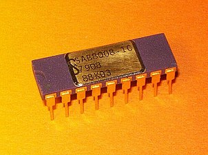 Siemens SAB8008


See also edit
- Intel Intellec 8
- Mark-8 and SCELBI, 8008-based computer kits
- MCM/70 and Micral, pioneering microcomputers
- PL/M, the first programming language targeting a microprocessor, the Intel 8008, developed by Gary Kildall
Notes edit
- ^ CPZS flags are presented as a group in this order during state 4 of the PCC cycle of the INP instruction.
References edit
External links edit
- MCS-8 User Manual with 8008 data sheet (1972)
- Wood, Lamont (2008-08-08). "Forgotten PC history: The true origins of the personal computer". Computer World.
- The Intel 8008 support page unofficial
- The DigiBarn Computer Museum's page on Bill Pentz' Sacramento State machine, a full microcomputer built around the 8008
- Martin, Donald P. (1974). Microcomputer Design. Martin Research.
- — (1976). Microcomputer Design (2 ed.). Martin Research. OCLC 911808003.
- Runyan, Grant (April 1977). "Now — BASIC for the 8008 — Even!". Kilobaud Magazine: 116–118.
- "A BASIC language interpreter for the Intel 8008 microprocessor". University of Illinois. 1974.
- 8008 Assembly Language Reference Card
- Shirriff, Ken (December 2016). "Die photos and analysis of the revolutionary 8008 microprocessor, 45 years old".
- — (February 2017). "Reverse-engineering the surprisingly advanced ALU of the 8008 microprocessor".
- — (October 2020). "How the bootstrap load made the historic Intel 8008 processor possible".
- — (November 2020). "Reverse-engineering the carry-lookahead circuit in the Intel 8008 processor".